Building the Foundation for a Smarter World
Semiconductor Manufacturing Solutions
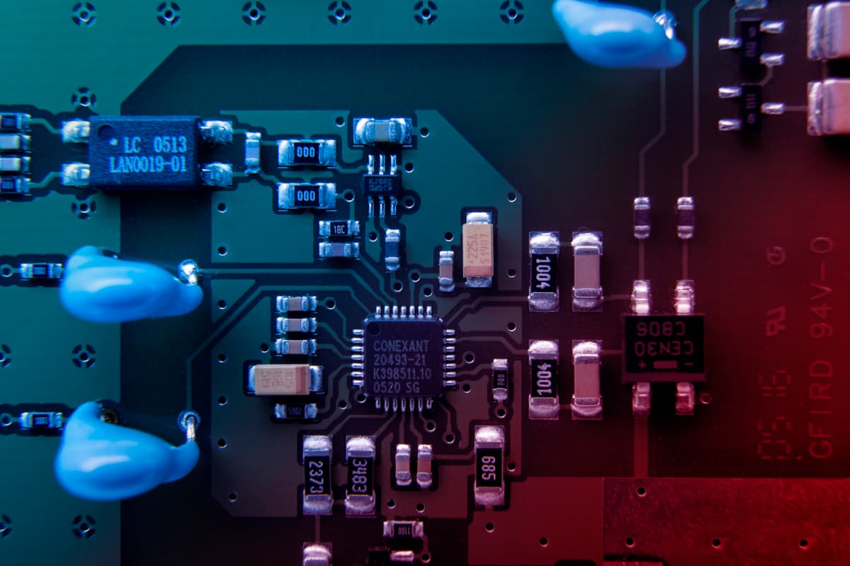
Semiconductor
Building the Foundation for a Smarter World

The semiconductor industry requires precision manufacturing, contamination-controlled production environments, and highly reliable equipment integration. Flexi Versa Group combines semiconductor machining, cleanroom manufacturing, and advanced assembly capabilities to support semiconductor equipment manufacturers, and lithography tool assembly programmes
Our Semiconductor Manufacturing Capabilities
Delivering Excellence in Semiconductor Solutions
Our capabilities support lithography tools assembly, semiconductor capital equipment, precision mechanical assemblies, cable harnesses, and cleanroom-built systems requiring high accuracy and contamination-controlled manufacturing environments. We combine global expertise, cutting-edge innovation, and a customer-first approach to deliver solutions that set new standards in semiconductor manufacturing.
Customised Manufacturing Solutions
Tailored manufacturing solutions designed to meet the specific requirements of semiconductor modules, including semiconductor machining, equipment assembly, cable integration, and cleanroom manufacturing processes for complex capital equipment applications.
Positioned for Semiconductor Supply Chain Access
Strategic presence in Asia and North America enables global support for equipment manufacturers, supporting regional and global semiconductor equipment manufacturers through strategic manufacturing locations and supply chain connectivity.
Semiconductor Tools Manufacturing Excellence
Cleanroom assembly and integration of lithography tools with stringent process controls to ensure reliability and precision.
Intellectual Property Management
IP protection ensured through ISO 27001 certification, secure infrastructure, and strong governance protocols.
Our Proven Solutions
Innovating Semiconductor Manufacturing Through Global Collaboration
In partnership with our global network, we provide vertically integrated manufacturing solutions for the semiconductor industry. From high-precision machining and cable assemblies to cleanroom systems, we meet the demands of capital equipment manufacturing. Strategically located near semiconductor ecosystems and continuously expanding our capabilities, we enable our customers to accelerate innovation and gain a competitive advantage.
Lithography Machines
We specialise in assembly, repair, and upgrading lithography tools to ensure maximum performance, high reliability, and extended equipment lifecycle for the semiconductor and electronics manufacturing industries. Our solutions enhance tool accuracy, operational efficiency, and uptime, supporting mission-critical fabrication processes and high-yield semiconductor production.
Metal Solutions for Lithography Tools
We deliver high-precision machined components and custom fabricated metal parts engineered specifically for lithography tools in the semiconductor and electronics manufacturing industries (supported by semiconductor CNC machining capabilities and precision fabrication processes). Our solutions ensure structural integrity, tight tolerances, and high-performance integration, supporting reliable, mission-critical equipment operation and optimised fabrication processes.
Bundled Cable Harness Solutions
We design and manufacture bundled cable assemblies engineered for signal integrity, durability, and seamless integration in semiconductor lithography systems. Each assembly is rigorously tested in cleanroom environments to ensure reliable performance, long-term operational stability, and compliance with mission-critical standards. Our solutions support complex semiconductor equipment, high-precision fabrication, optimised tool functionality, automated manufacturing systems, and maintenance-free operation.
Clean Room Assemblies
We provide precision assembly services in ISO Class 7 and 8 cleanrooms for semiconductor lithography equipment, integrating leakage control, alignment, and calibration processes to achieve stringent mechanical tolerances, high accuracy, and reliable tool performance. Our solutions ensure mission-critical equipment integrity, optimised fabrication processes, and long-term operational stability for the semiconductor and high-tech manufacturing industries.
Semiconductor
Why Cleanroom Manufacturing Matters in Semiconductor Production
Semiconductor equipment manufacturing requires strict contamination control to maintain equipment performance, process reliability, and product quality. Cleanroom manufacturing environments help minimise airborne particles, contaminants, and process variability that could impact precision equipment and semiconductor fabrication processes. Flexi Versa Group's cleanroom manufacturing capabilities include: • ISO Class 7 cleanroom manufacturing • ISO Class 8 cleanroom manufacturing • Precision cleanroom assembly • Semiconductor equipment integration • Calibration and validation activities • Contamination-controlled production workflows
Case Study: 3D Printer Precision Box Build with Embedded Electronics
Case Study: 3D Printer Precision Box Build with Embedded Electronics
A customer needed to commercialise a complex 3D printing system while running NPI in parallel across multiple design teams. With no internal manufacturing capability, the entire build had to be executed externally under strict budget and timeline constraints.
FVG deployed subject matter experts in metals, electronics, wiring, and system integration directly at the client’s R&D hub to support problem solving and process scale-up. By leveraging Malaysia’s robust manufacturing ecosystem, FVG established a flexible build platform that supported both design evolution and commercialisation.
Manufacturing Process:
System Integration: Full mechanical assembly with embedded electronics, wiring, and metal structures.
Collaboration: On-site engineering support to align R&D and production scale-up.
Box Build Solution: A complete end-to-end build platform capable of evolving alongside product design requirements.
Outcome:
FVG delivered the full NPI build in just 4 weeks by combining DVT and PVT cycles, supported by a cross-functional team of specialists. The project achieved cost targets of US$100K per unit, well below the industry benchmark of US$200K–800K. Just as important, the production framework was designed with foresight, so the path from prototype to higher volumes was already in place.
Insights
Gain Access Into Our Team’s Perspectives and Insights on the Topic
Frequently Asked Questions
FAQs
What semiconductor manufacturing solutions does Flexi Versa Group provide?
Yes. At Flexi Versa Group, we provide semiconductor machining, cleanroom manufacturing, lithography tool assembly, cable harness integration, and semiconductor equipment assembly solutions.
Does Flexi Versa Group provide semiconductor CNC machining services?
Yes. We provide precision machining capabilities for semiconductor equipment, lithography systems assembly, and high-precision industrial applications.
What cleanroom manufacturing capabilities does Flexi Versa Group provide?
Flexi Versa Group operates ISO Class 7 (10,000 Cleanroom) and ISO Class 8 (100,000 Cleanroom) environments for semiconductor manufacturing and assembly applications.
What types of semiconductor equipment does Flexi Versa Group support?
Capabilities include lithography systems assembly, precision mechanical assemblies, cable harnesses, cleanroom-built equipment, and semiconductor manufacturing tools.
Why is cleanroom manufacturing important in semiconductor production?
Cleanroom manufacturing helps minimise contamination, maintain equipment precision, and improve manufacturing consistency for semiconductor applications.
What is the difference between ISO Class 7 and ISO Class 8 cleanrooms?
ISO Class 7 and ISO Class 8 cleanrooms maintain controlled airborne particle levels, with ISO Class 7 providing stricter contamination control requirements.
Can Flexi Versa Group support NPI and production scale-up for semiconductor equipment?
Yes. We support new product introduction (NPI), engineering validation, and scalable production frameworks for complex equipment manufacturing.
Does Flexi Versa Group provide box build solutions for semiconductor equipment?
Yes. We provide complete box build solutions involving mechanical structures, embedded electronics, wiring integration, and system-level assembly.