news
Process - Wave Soldering: Ensuring Precision and Reliability in PCB Assembly
/)
What is Wave Soldering?
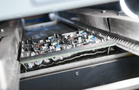
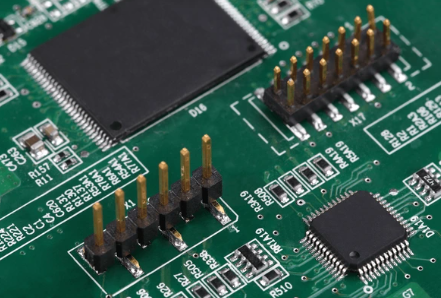
Wave soldering is a process where a PCB is passed over a flowing wave of molten solder, allowing the solder to attach components to the board. The board is first preheated, fluxed, and cleaned to promote proper wetting and adhesion. It is particularly effective for through-hole components, although it can also assist in mixed-technology boards (with surface-mount components pre-placed).
Common Wave Soldering Defects
Even in experienced facilities, several defects can occur if the process is not tightly controlled:
Solder Bridges
Occur when solder connects two adjacent pads unintentionally.
Often caused by excessive solder, misaligned components, or improper board design.
Cold Joints
Result from insufficient heat or poor wetting of solder on the pads and leads.
Leads to weak electrical connections and potential failures in the field.
Insufficient Wetting
When solder fails to properly coat component leads or pads.
Causes poor mechanical and electrical connections.
Component Misalignment or Tombstoning
Components may lift or tilt during soldering, creating improper contact with pads.
Often caused by uneven heating or solder surface tension issues.
Solder Balls / Spattering
Tiny solder droplets form on the board surface, often due to excessive flux, improper wave height, or high preheat temperature.
Can create short circuits or cosmetic defects.
Flux Residue or Oxidation
Residual flux or surface oxidation reduces solder quality and can affect long-term reliability.
Control Measures in Place
At advanced manufacturing facilities, strict process controls and preventive measures are applied to minimise defects:
Optimised Solder Parameters
Temperature, wave height, and conveyor speed are precisely controlled for consistent soldering.
Fluxing Control
Proper flux type and application ensure good wetting and reduce oxidation.
Preheating and Board Conditioning
Boards are preheated to reduce thermal shock and prevent cold joints or tombstoning.
Component Placement and Board Design
Proper pad sizing, spacing, and component alignment reduce the risk of bridging or misalignment.
Wave Maintenance
Regular maintenance of the solder wave, including filtration and dross removal, ensures consistent solder quality.
Inspection and Quality Checks
Automated optical inspection (AOI) and manual checks identify defects early.
Rework stations allow immediate correction of minor defects.
Training and Standard Operating Procedures (SOPs)
Operators are trained to monitor process variations and intervene before defects escalate.
The Result: Reliable, High-Quality PCB Assembly
By combining controlled wave soldering parameters, proper board preparation, and rigorous inspection, manufacturers can minimise defects, improve first-pass yield, and deliver reliable PCBs for critical applications.
Wave soldering is more than just a production step — it is a process that demands precision, control, and continuous improvement. With the right measures in place, it remains a highly efficient and dependable method for producing high-quality electronic assemblies, whether for industrial, consumer, or medical devices.
Contact us to find out more.